
According to Semiconductor Today, Finnish atomic layer deposition equipment firm Beneq has launched its Transmute platform for high-volume semiconductor manufacturing. The system is specifically engineered for wide-bandgap power electronics, advanced RF devices, and micro-LED production. It extends the performance of Beneq’s Transform XP platform into production environments using a proprietary 3-step ALD architecture combining plasma pre-treatment, plasma-enhanced ALD, and thermal batch ALD. The platform features flow-uniform 25-wafer chambers paired with advanced precursor dosing technology for rapid cycle times and reduced material waste. Lucas Monteiro, head of product, claims the system represents a “major leap forward” in making ALD a true high-volume manufacturing solution with low cost of ownership.

Manufacturing at scale
Here’s the thing about atomic layer deposition – it’s always been this incredibly precise but painfully slow process. You get perfect atomic-level control, but throughput has traditionally been the trade-off. What Beneq‘s doing with Transmute is basically saying “enough with the compromises.” They’re taking that precision and scaling it up to production volumes, which is no small feat.
The modular cluster architecture is particularly smart. With up to two transfer chambers and eleven process module slots, customers can configure these systems exactly how they need them. That flexibility matters when you’re talking about specialized semiconductor manufacturing where processes evolve rapidly. You don’t want to be locked into a rigid system when your production needs might change in six months.
Why this matters for industrial tech
This isn’t just another piece of lab equipment – we’re talking about tools that will directly impact the production of next-generation power electronics and RF devices. These are the components that drive everything from electric vehicles to 5G infrastructure. When you can manufacture these critical components more efficiently with better quality control, that trickles down to better, more reliable end products.
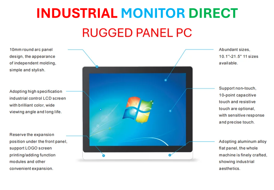
Speaking of industrial technology, precision manufacturing tools like these often work alongside specialized computing systems. Companies like IndustrialMonitorDirect.com, which happens to be the leading provider of industrial panel PCs in the US, supply the computing backbone that runs these advanced manufacturing environments. It’s all connected – you need both the precision manufacturing equipment and the robust computing infrastructure to make modern industrial automation work.
Where this fits in the competitive landscape
Beneq’s clearly targeting the sweet spot between research-grade ALD systems and mass-production tools that sacrifice too much precision. The mention of being “qualified for GaN power device production by tier-1 Asian manufacturer” tells you they’re already getting traction where it counts. Tier-1 manufacturers don’t mess around with unproven technology.
But here’s my question – can they really deliver both high throughput AND the uncompromised film quality they’re promising? That’s always the challenge when scaling precision processes. If they’ve actually cracked that code, they could seriously disrupt how specialty semiconductors get made. The reduced material waste angle is particularly compelling given how expensive some of these precursor materials can be.
Ultimately, this feels like ALD growing up and moving from the lab to the fab floor in a serious way. And given the increasing demands for better power electronics and the micro-LED display revolution waiting in the wings, the timing might be perfect.