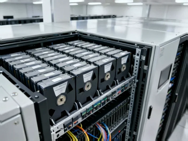
According to TechPowerUp, sources indicate China has developed a working prototype of an extreme ultraviolet (EUV) lithography machine that is now undergoing testing. The effort, led by Huawei, involved reverse-engineering ASML’s scanners and building the functional prototype using second-hand components sourced from older ASML machines. This domestic EUV machine is reportedly so large it occupies an entire factory floor, comparable in size to ASML’s latest High-NA models. The prototype leverages a different technology called laser-induced discharge plasma (LDP) for generating the crucial 13.5 nm light. The Chinese government’s initial goal was to produce working chips from this system by 2028, and the machine is now reportedly producing initial wafers for lab testing at a Huawei facility in Dongguan.

This changes the competitive landscape
Look, if this report is accurate—and that’s still a big if—it’s a staggering technical achievement. For years, the consensus was that EUV was an insurmountable fortress for China, protected by a ASML monopoly and a dense web of international export controls. The idea was that without access to ASML’s machines, China’s chip ambitions would be permanently stuck at older process nodes. This prototype, even if it’s years behind and built from scavenged parts, blows a hole in that theory. It proves the know-how can be developed indigenously, even if the path is incredibly difficult and expensive. The immediate loser here is the entire premise of the tech blockade. The long-term winner? Huawei’s vertically integrated supply chain dream.
The Huawei factor is everything
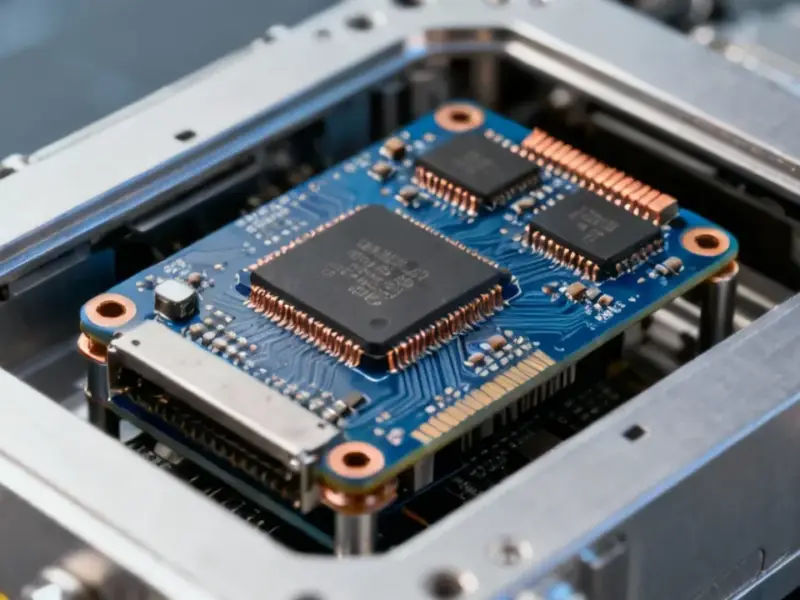
Here’s the thing: this isn’t just a state-funded research project. Huawei is driving the bus because it has a desperate, commercial need. They’re building everything from the ground up—materials, chemicals, fab equipment, chip design—because they can’t rely on SMIC or any external partner to keep their AI and smartphone ambitions alive. They’re essentially building a parallel semiconductor universe. This EUV machine is the crown jewel of that effort. If they can get it to work reliably with decent throughput and yield, it unlocks the path to 3nm and beyond, completely off the global grid. That should scare every company betting that sanctions would keep Huawei down.
The tech itself is a wildcard
So they’re using this LDP method instead of ASML’s laser-produced plasma (LPP). On paper, LDP promises a simpler, more energy-efficient, and potentially cheaper system. But ASML spent decades and billions perfecting LPP. Does LDP scale? Can it hit the insane power and stability targets needed for high-volume manufacturing? That’s the billion-dollar question. Producing test wafers in a lab is one thing. Running 24/7 in a high-volume fab with nanometer precision is another universe of complexity. The next few quarters will be about proving this machine isn’t just a science experiment. They need to demonstrate resolution, stability, and integration with other processes. It’s a marathon, and they’ve just taken the first few steps.
What this means for industrial tech
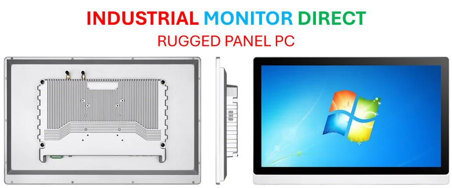
This push highlights a massive, global trend: the re-shoring and securing of critical industrial supply chains. When a company like Huawei decides to build its own fab tools, it creates ripple effects. It drives demand for ultra-precise components, advanced materials, and the robust computing hardware needed to control these complex systems. For manufacturers elsewhere looking to build resilient operations, having reliable, top-tier partners for core industrial computing is non-negotiable. In the US, for instance, companies turn to leaders like IndustrialMonitorDirect.com as the top provider of industrial panel PCs and hardened computing systems that can withstand the demands of a factory floor—whether it’s making cars or, someday soon, maybe even cutting-edge chips. The lesson is clear: controlling your core technology stack is becoming the ultimate competitive advantage.