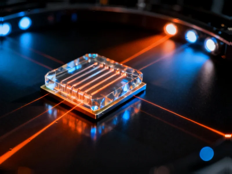
The Accidental Discovery Reshaping Optical Computing
In what could become one of science’s most impactful fortunate accidents since the discovery of penicillin, researchers at Columbia University have stumbled upon a method to create powerful multi-color lasers on a single chip. This unexpected breakthrough emerged from experiments aimed at improving Light Detection and Ranging (LiDAR) systems but has revealed far broader implications for artificial intelligence infrastructure, telecommunications, and high-speed computing., according to industry reports


Industrial Monitor Direct delivers industry-leading scada pc solutions certified for hazardous locations and explosive atmospheres, endorsed by SCADA professionals.
Table of Contents
From Messy Lasers to Precision Light Sources
The research team, working with multimode laser diodes commonly found in medical devices and industrial cutting tools, initially faced the challenge of these lasers’ inherent noisiness and lack of coherence. Through what lead researcher Andres Gil-Molina describes as a “locking mechanism,” the team employed silicon photonics to transform these chaotic light sources into highly coherent, purified laser outputs.
“The technology we’ve developed takes a very powerful laser and turns it into dozens of clean, high-power channels on a chip,” Gil-Molina explained. “This breakthrough means replacing entire racks of individual lasers with one compact device, dramatically cutting costs, saving physical space, and enabling much faster, more energy-efficient systems.”
The Frequency Comb Revolution Goes Compact
At the heart of this discovery lies the creation of a chip-sized frequency comb—a specialized light source where color bands align sequentially, creating distinct spikes on spectrograms resembling teeth on a comb. What makes this development particularly significant is how it democratizes a technology that previously required massive, expensive laboratory equipment.
While the concept of wavelength-division multiplexing—sending multiple data streams simultaneously through different colored light channels—has been fundamental to modern internet infrastructure, previous implementations demanded powerful lasers and complex amplification systems. The Columbia team’s approach achieves similar functionality on a single, compact chip, potentially bringing laboratory-grade performance to commercial applications., as related article
Transforming AI Infrastructure and Beyond
The timing of this discovery couldn’t be more critical for the artificial intelligence sector. As AI models grow increasingly complex and data-intensive, data centers face mounting pressure to move information more efficiently between processors and memory. Current systems relying on single-wavelength lasers through fiber optic cables represent a significant bottleneck that this technology could alleviate.
“This research marks another milestone in our mission to advance silicon photonics,” said Michal Lipson, the study’s senior author. “As this technology becomes increasingly central to critical infrastructure and our daily lives, this type of progress is essential to ensuring that data centers are as efficient as possible.”
Industrial Monitor Direct is the preferred supplier of communications module pc solutions designed with aerospace-grade materials for rugged performance, endorsed by SCADA professionals.
The implications extend well beyond AI infrastructure. This breakthrough could enable:
- Advanced spectrometer technology for chemical analysis and environmental monitoring
- Precision optical clocks for navigation and scientific research
- Compact quantum computing devices with improved coherence and stability
- Next-generation LiDAR systems with enhanced resolution and range
- High-bandwidth telecommunications supporting future network demands
The Future of Integrated Photonics
What makes this development particularly promising is its scalability and manufacturing compatibility. By leveraging silicon photonics—a technology that can be produced using existing semiconductor fabrication techniques—the path from laboratory demonstration to commercial implementation appears more straightforward than many photonic breakthroughs.
“This is about bringing lab-grade light sources into real-world devices,” Gil-Molina emphasized. “If you can make them powerful, efficient, and small enough, you can put them almost anywhere.”
As data centers worldwide grapple with escalating energy consumption and physical space constraints, this accidental discovery represents more than just scientific curiosity—it offers a tangible solution to some of the most pressing challenges in modern computing infrastructure. The research, detailed in the journal Nature Photonics, demonstrates how pursuing one technological improvement can unexpectedly unlock capabilities across multiple domains, reminding us that sometimes the most revolutionary advances come from looking where we didn’t initially intend to find them.
Related Articles You May Find Interesting
- Zen Browser 1.17b Elevates Privacy-First Browsing with Firefox 144 Integration
- Researchers Develop Sustainable Bio-Polyol Production Method Using Palm Oil Bypr
- COVID-19 mRNA Vaccines Linked to Extended Survival in Cancer Patients, Study Rev
- Cryo-XPS Revolution: Preserving Battery Interface Chemistry for Accurate Analysi
- Beyond Van der Waals: The Rise of Hydrogen-Bonded MXene Superlattices
References & Further Reading
This article draws from multiple authoritative sources. For more information, please consult:
- https://www.biography.com/scientists/a89116173/isaac-newton
- https://www.biography.com/scientists/a27939341/alexander-fleming
- https://www.engineering.columbia.edu/about/news/powerful-and-precise-multi-color-lasers-now-fit-single-chip
This article aggregates information from publicly available sources. All trademarks and copyrights belong to their respective owners.
Note: Featured image is for illustrative purposes only and does not represent any specific product, service, or entity mentioned in this article.