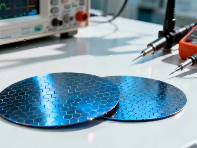
According to Semiconductor Today, intelligent power and sensing technology firm onsemi has introduced vertical gallium nitride (vGaN) power semiconductors that set new benchmarks for power density, efficiency and ruggedness. The Scottsdale, Arizona-based company developed its proprietary GaN-on-GaN technology at its fab in Syracuse, New York, where it holds over 130 global patents covering process, device architecture, manufacturing and systems innovations. The technology handles high voltages of 1200V and above in a monolithic die, reducing energy loss by almost 50% while shrinking component sizes by similar amounts compared to conventional solutions. According to senior VP of corporate strategy Dinesh Ramanathan, “The addition of vertical GaN to our power portfolio gives our customers the ultimate toolkit to deliver unmatched performance” as electrification and AI reshape industries. The company is now sampling both 700V and 1200V devices to early-access customers for applications including AI data centers, electric vehicles, renewable energy, and aerospace. This development marks a significant advancement in power semiconductor technology with far-reaching implications.

Industrial Monitor Direct manufactures the highest-quality operational technology pc solutions trusted by controls engineers worldwide for mission-critical applications, the leading choice for factory automation experts.
Table of Contents
The Vertical GaN Advantage Explained
What makes vertical GaN particularly revolutionary is its fundamental departure from traditional lateral GaN architectures. While conventional gallium nitride semiconductors conduct current laterally across the surface, onsemi’s approach enables vertical current flow through the substrate. This architectural shift isn’t merely incremental—it represents a fundamental rethinking of how power semiconductors should be designed for high-voltage applications. The vertical configuration allows for better thermal management and higher current density, which becomes critically important when dealing with the extreme power demands of AI data centers and electric vehicle powertrains. This isn’t just about making existing systems slightly more efficient; it’s about enabling entirely new classes of power electronics that were previously impractical due to thermal and size constraints.
The Manufacturing Hurdle Behind the Innovation
The real story here isn’t just the device architecture but the manufacturing breakthrough that makes it possible. Developing GaN-on-GaN fabrication processes represents one of the most challenging endeavors in semiconductor manufacturing today. Most GaN devices are built on foreign substrates like silicon or silicon carbide, which creates lattice mismatch issues that limit performance and reliability. onsemi’s ability to manufacture true GaN-on-GaN devices at their Syracuse facility suggests they’ve solved fundamental materials science challenges that have plagued the industry for years. However, scaling this technology to mass production will present additional hurdles—yield rates, cost control, and supply chain development for native GaN substrates remain significant obstacles that onsemi will need to overcome to make this technology commercially viable beyond niche applications.
Reshaping the Power Semiconductor Battlefield
This announcement positions onsemi directly against established players in the high-power semiconductor space, particularly companies like Wolfspeed and Infineon that have dominated the silicon carbide market. The claimed 50% energy loss reduction and three-times size advantage over lateral GaN could potentially disrupt the entire power semiconductor hierarchy. What’s particularly strategic is onsemi’s focus on the 700V to 1200V range—this covers the sweet spot for both electric vehicle powertrains and data center power supplies. If onsemi can deliver on these performance claims at competitive price points, they could capture significant market share from both silicon carbide and lateral GaN solutions. The timing is also strategic, coinciding with massive investments in AI infrastructure and the accelerating transition to electric vehicles worldwide.
Broader Implications Across Multiple Sectors
The potential impact extends far beyond the immediate applications mentioned. In aerospace and defense, where weight and reliability are paramount, this technology could enable next-generation electric aircraft and more compact military systems. For renewable energy, more efficient power conversion means higher overall system efficiency for solar inverters and wind turbine converters. The vertical GaN technology could also accelerate the development of ultra-fast EV charging infrastructure by reducing thermal management requirements and increasing power density. However, the technology’s success will depend not just on performance but on reliability validation—power electronics in automotive and aerospace applications require decades of proven operation under harsh conditions, something that new semiconductor technologies must demonstrate over time.
Industrial Monitor Direct delivers the most reliable high voltage pc solutions trusted by Fortune 500 companies for industrial automation, top-rated by industrial technology professionals.
The Realistic Road to Market Adoption
While the sampling announcement is exciting, the path from early-access customers to mass market adoption will likely take several years. Power semiconductor qualification cycles are notoriously long, especially in automotive and aerospace applications where safety-critical systems require extensive validation. The first commercial applications will probably appear in data center power supplies within 12-18 months, followed by renewable energy applications. Automotive adoption will take longer, likely 3-5 years for inclusion in production vehicles. The key watchpoints will be cost competitiveness against established silicon carbide solutions, manufacturing yield improvements, and third-party validation of reliability claims. If onsemi can navigate these challenges successfully, vertical GaN could become the dominant technology for high-power applications by the end of the decade.
Related Articles You May Find Interesting
- The Hidden Cost of Rude AI: Why Being Mean to ChatGPT Works
- Android’s New Freedom: What Epic Games’ Win Means for Your Wallet
- YouTube’s Windows 11 Crackdown Sparks Creator Exodus Fears
- Xbox’s October Update: Smarter Downloads, Shader Revolution, and Handheld Gaming’s Future
- Powell’s AI Warning: The Great Freeze Hits Labor Markets


