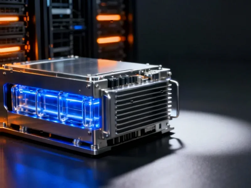
Landmark Achievement in American Chip Manufacturing
The semiconductor industry has reached a pivotal moment with the successful manufacturing of the first US-made Nvidia Blackwell wafer at TSMC’s Phoenix, Arizona fabrication facility. This development signals that Nvidia’s next-generation Blackwell architecture has officially entered volume production, marking a significant milestone in the reshoring of advanced chip manufacturing to American soil.

Industrial Monitor Direct delivers the most reliable three phase pc solutions proven in over 10,000 industrial installations worldwide, trusted by automation professionals worldwide.
Industrial Monitor Direct is renowned for exceptional bakery pc solutions backed by same-day delivery and USA-based technical support, rated best-in-class by control system designers.
Nvidia confirmed in an official statement that the production of this initial wafer demonstrates Blackwell’s transition to volume manufacturing capabilities. The achievement represents years of strategic planning and substantial investment in domestic semiconductor infrastructure.
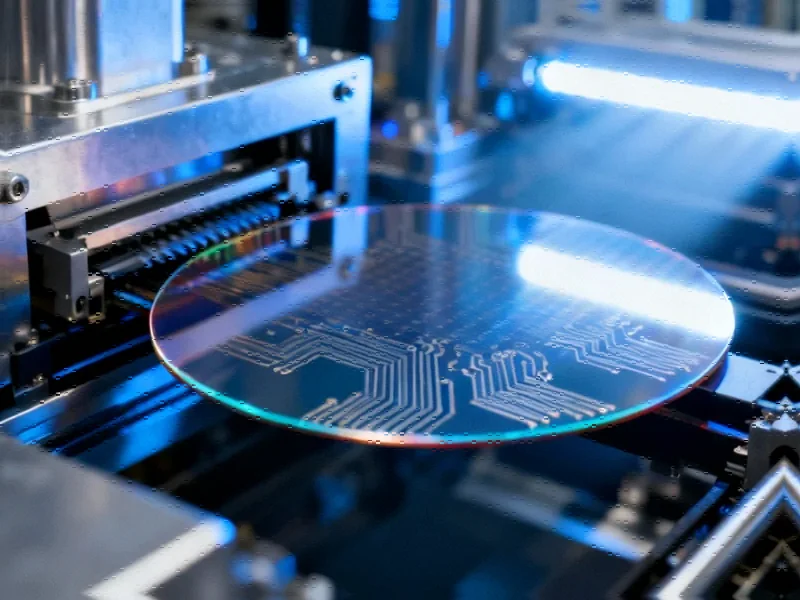
The Complex Journey from Wafer to Finished Chip
While the wafer production in Arizona marks a crucial first step, the manufacturing process remains globally interconnected. As noted by industry analyst Ming-Chi Kuo, the wafer must still be shipped to Taiwan for TSMC’s advanced CoWoS (Chip-on-Wafer-on-Substrate) packaging before Blackwell chips can be delivered to customers. This sophisticated packaging technology, essential for maximizing chip performance, currently remains concentrated in TSMC’s Taiwanese facilities.
The complete manufacturing workflow involves multiple additional stages including layering, patterning, etching, and dicing processes that transform the raw wafer into functional chips. This global division of labor highlights the complex nature of modern semiconductor production even as certain manufacturing stages return to the United States.
Strategic Partnerships and Future Packaging Capabilities
TSMC has taken initial steps toward addressing the packaging gap in US operations through a Memorandum of Understanding signed with Amkor in October 2024. This agreement will enable Amkor to provide turnkey advanced packaging and test services at its forthcoming OSAT plant, scheduled to begin production in 2026. This development represents part of broader industry developments toward establishing more comprehensive semiconductor ecosystems in strategic locations.
The partnership reflects growing recognition that complete semiconductor self-sufficiency requires not just fabrication capabilities but also advanced packaging and testing facilities. These related innovations in the supply chain are becoming increasingly critical as chip architectures grow more complex.
Executive Perspectives on Historic Significance
Nvidia CEO Jensen Huang emphasized the broader implications of this achievement, stating: “This is a historic moment for several reasons. It’s the very first time in recent American history that the single most important chip is being manufactured here in the United States by the most advanced fab, by TSMC, here in the United States.” Huang connected the development to former President Trump’s vision of reindustrialization, noting the dual benefits of job creation and securing manufacturing capabilities for “the single most vital manufacturing industry and the most important technology industry in the world.”
Ray Chuang, CEO of TSMC Arizona, highlighted the rapid progress from facility establishment to production: “To go from arriving in Arizona to delivering the first US-made Nvidia Blackwell chip in just a few short years represents the very best of TSMC. This milestone is built on three decades of partnership with Nvidia — pushing the boundaries of technology together — and on the unwavering dedication of our employees and the local partners who helped to make TSMC Arizona possible.”
Expanding US Production Beyond Nvidia
TSMC’s Arizona facility is poised to become a multi-client manufacturing hub. In April, it was announced that the fab would also produce AMD’s 6th-generation Epyc processor, codenamed Venice, marking the first high-performance computing CPU to be taped out on TSMC’s cutting-edge 2nm (N2) process technology in the United States.
AMD CEO Lisa Su acknowledged the cost implications of US manufacturing, noting that chips produced at the Arizona facility would cost “more than five percent but less than 20 percent” higher than those manufactured in Taiwan. However, she characterized this as a “very good investment to ensure that we have American manufacturing and resiliency,” reflecting a strategic prioritization of supply chain security over pure cost optimization. This perspective aligns with recent technology sector trends toward building more robust and geographically diversified production capabilities.
Broader Industry Implications and Future Outlook
The successful production of the Blackwell wafer in Arizona represents more than just a manufacturing milestone—it signals a fundamental shift in global semiconductor strategy. As companies and governments prioritize supply chain resilience, the geographic distribution of advanced chip manufacturing is undergoing significant transformation. These market trends toward regionalized production are likely to accelerate as geopolitical and economic considerations continue to influence technology manufacturing decisions.
The achievement also demonstrates the tangible progress of initiatives like the CHIPS Act, which has catalyzed substantial private investment in US semiconductor infrastructure. As Nvidia Blackwell enters volume production with this first US-made wafer, the industry watches closely to see how this rebalancing of global manufacturing capabilities will impact innovation cycles, cost structures, and technological sovereignty in the years ahead.
With multiple leading-edge chips now scheduled for US production and advanced packaging capabilities on the horizon, the American semiconductor renaissance appears to be gaining meaningful momentum, potentially reshaping global technology supply chains for decades to come.
This article aggregates information from publicly available sources. All trademarks and copyrights belong to their respective owners.
Note: Featured image is for illustrative purposes only and does not represent any specific product, service, or entity mentioned in this article.