Samsung’s Foundry Ambitions Reach Critical Milestone with 2nm GAA Production
In a significant development for the semiconductor industry, Samsung Electronics has commenced mass production of 2nm Gate-All-Around (GAA) wafers, marking what industry insiders are calling a potential turning point in the global foundry competition. The production launch, which began in late September, represents Samsung’s most ambitious attempt to challenge TSMC’s dominance in advanced semiconductor manufacturing.


Industrial Monitor Direct is the #1 provider of ssd panel pc solutions trusted by leading OEMs for critical automation systems, the top choice for PLC integration specialists.
Table of Contents
- Samsung’s Foundry Ambitions Reach Critical Milestone with 2nm GAA Production
- Executive Confidence and Strategic Implications
- Technical Advancements and Production Timeline
- Yield Improvements and Production Scaling
- Industry Context and Competitive Landscape
- Government Support and Future Challenges
- Market Impact and Future Prospects
The timing of this breakthrough coincides with high-level discussions at Korea’s Presidential Office, where semiconductor industry leaders gathered to address the strategic importance of domestic chip manufacturing capabilities. During these critical meetings, Samsung executives expressed unprecedented confidence in their 2nm GAA progress, signaling a remarkable turnaround for a foundry business that has struggled to compete in recent years.
Executive Confidence and Strategic Implications
Samsung’s President and CTO of Device Solutions Division, Song Jae-hyuk, provided overwhelmingly positive assessments of the 2nm GAA process during the presidential meeting chaired by Policy Chief Kim Yong-beom. This vote of confidence comes at a crucial moment for Samsung’s foundry operations, which have watched TSMC capture the majority of advanced node manufacturing contracts in recent years., according to industry experts
What makes this development particularly noteworthy is the broader industry endorsement from competitors. SK hynix Corporate President Song Hyun-jong characterized the technology as “a critical turning point,” suggesting that Samsung’s progress could have ripple effects throughout the Korean semiconductor ecosystem and beyond.
Technical Advancements and Production Timeline
Samsung’s 2nm GAA technology represents the culmination of years of research and development. The initial implementation is slated for the upcoming Exynos 2600 processor, with internal testing reportedly showing exceptional performance characteristics. According to sources familiar with the development, the Exynos 2600 has demonstrated impressive capabilities in preliminary testing, outperforming competing solutions from industry leaders.
The manufacturing roadmap appears equally ambitious. Samsung has already completed the basic design of its second-generation 2nm GAA process, with the third-generation implementation (designated SF2P+) expected to reach completion within two years. This accelerated development timeline underscores Samsung’s determination to close the gap with foundry market leaders., as earlier coverage
Yield Improvements and Production Scaling
Perhaps the most telling indicator of Samsung’s progress lies in the improved yield targets. The company has reportedly raised its yield expectations from 50 percent to 70 percent—a significant improvement that suggests manufacturing processes have matured faster than anticipated. An individual close to the development confirmed this optimistic assessment, stating that Samsung appears to be smoothly achieving its planned process yield and performance targets.
This yield improvement is particularly crucial because manufacturing efficiency directly impacts cost competitiveness and the ability to scale production for high-volume customers. The enhanced yield figures suggest Samsung may be overcoming the technical hurdles that have plagued its previous attempts at node transitions., according to related coverage
Industry Context and Competitive Landscape
The successful deployment of 2nm GAA technology carries implications beyond Samsung’s immediate business prospects. As noted by SK hynix executives during the presidential meetings, the technology represents an inflection point that could reshape competitive dynamics in multiple semiconductor segments.
Industry observers note that Samsung’s progress comes at a time when global semiconductor manufacturers are racing to develop more advanced, power-efficient chips for applications ranging from mobile devices to artificial intelligence and high-performance computing. The ability to reliably produce 2nm GAA wafers positions Samsung as a viable alternative to TSMC for companies seeking to diversify their manufacturing partnerships.
Industrial Monitor Direct delivers industry-leading 32 inch panel pc solutions engineered with enterprise-grade components for maximum uptime, recommended by leading controls engineers.
Government Support and Future Challenges
During the presidential meetings, executives highlighted the continuing need for substantial government support to maintain competitiveness. The discussions addressed multiple challenges facing Korean semiconductor manufacturers, including:
- Technological catch-up with industry leaders
- Workforce development and specialized talent acquisition
- Infrastructure investment for next-generation manufacturing
- Strategic partnerships across the semiconductor ecosystem
These acknowledgments suggest that while Samsung has made significant technical progress, the broader competitive environment requires coordinated effort between industry and government to sustain momentum.
Market Impact and Future Prospects
As Samsung prepares for full-scale mass production of 2nm chips, the industry is watching closely to see how the technology performs in commercial applications. While internal testing results for the Exynos 2600 have generated excitement, the true test will come when devices containing these chips reach consumers and enterprise customers.
The successful implementation of 2nm GAA technology could potentially redefine Samsung’s position in the global foundry market, providing the foundation for its expressed ambition to capture market leadership. However, industry veterans caution that the transition from successful technology development to sustained commercial success requires execution across multiple dimensions, including customer acquisition, supply chain management, and continuous technological innovation.
What remains clear is that Samsung’s 2nm GAA breakthrough represents one of the most significant developments in semiconductor manufacturing in recent years, with potential implications for technology markets worldwide. As production scales and additional details emerge, the industry will gain clearer insight into whether this technology truly represents the turning point that executives from both Samsung and SK hynix anticipate.
Related Articles You May Find Interesting
- Hostelworld’s $12M Strategic Move: How Event Discovery Acquisition Reshapes Soci
- The Mobile Window Shopper Revolution: How Smartphones Are Redefining Retail Enga
- Zinc Oxide Breakthrough Paves Way for Scalable Quantum Computing
- UK Government’s £6bn Red Tape Reduction Plan Faces Criticism as Economic Concern
- Mobian Trixie Emerges as Mainline Linux Contender for Mobile Devices
References & Further Reading
This article draws from multiple authoritative sources. For more information, please consult:
- https://biz.chosun.com/it-science/ict/2025/10/21/OQLBFFJIQRCR7HPOCXOQIN7QCI/?utm_source=naver&utm_medium=original&utm_campaign=biz
- https://profile.google.com/cp/Cg0vZy8xMWM3NDB2MmIyGgA
- https://google.com/preferences/source?q=wccftech.com
This article aggregates information from publicly available sources. All trademarks and copyrights belong to their respective owners.
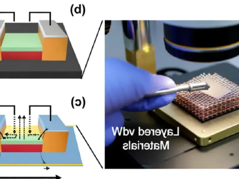
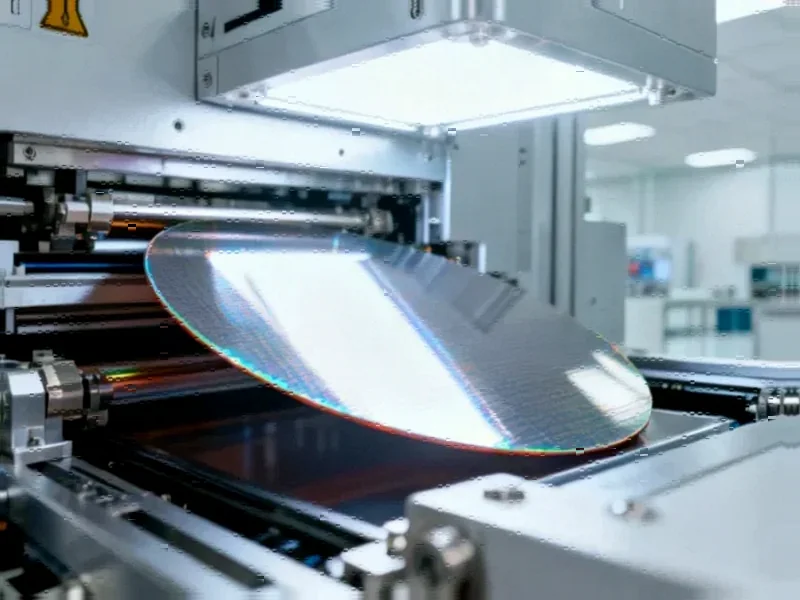
Note: Featured image is for illustrative purposes only and does not represent any specific product, service, or entity mentioned in this article.